- 您现在的位置:买卖IC网 > Sheet目录3753 > ATMEGA169P-16MCHR (Atmel)MCU AVR 16KB FLASH 16MHZ 64-VQFN
85
8018P–AVR–08/10
ATmega169P
13.3.7
Alternate Functions of Port G
The alternate pin configuration is as follows:
Note:
1. Port G, PG5 is input only. Pull-up is always on.
See Table 27-3 on page 297 for RSTDISBL fuse.
The alternate pin configuration is as follows:
RESET – Port G, Bit 5
RESET: External Reset input. When the RSTDISBL Fuse is programmed (‘0’), PG5 will function
as input with pull-up always on.
T0/SEG23 – Port G, Bit 4
T0, Timer/Counter0 Counter Source.
SEG23, LCD front plane 23
T1/SEG24 – Port G, Bit 3
T1, Timer/Counter1 Counter Source.
SEG24, LCD front plane 24
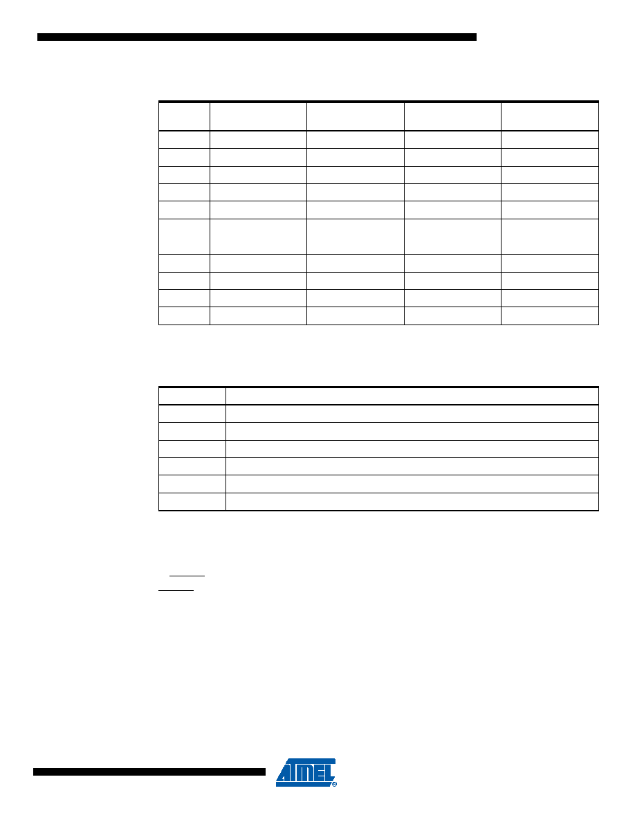
Table 13-20. Overriding Signals for Alternate Functions in PF3:PF0
Signal
Name
PF3/ADC3
PF2/ADC2
PF1/ADC1
PF0/ADC0
PUOE
0000
PUOV
0000
DDOE
0000
DDOV
0000
PVOE
0000
PVOV
0000
PTOE
––––
DIEOE
0000
DIEOV
0000
DI
––––
AIO
ADC3 INPUT
ADC2 INPUT
ADC1 INPUT
ADC0 INPUT
Table 13-21. Port G Pins Alternate Functions
Port Pin
Alternate Function
PG5
RESET
PG4
T0/SEG23 (Timer/Counter0 Clock Input or LCD Front Plane 23)
PG3
T1/SEG24 (Timer/Counter1 Clock Input or LCD Front Plane 24)
PG2
SEG4 (LCD Front Plane 4)
PG1
SEG13 (LCD Front Plane 13)
PG0
SEG14 (LCD Front Plane 14)
发布紧急采购,3分钟左右您将得到回复。
相关PDF资料
2-1546217-0
TERM BLK RCPT 20POS SIDE 5.08MM
1-1546217-9
TERM BLK RCPT 19POS SIDE 5.08MM
1-1546217-8
TERM BLK RCPT 18POS SIDE 5.08MM
1-1546217-7
TERM BLK RCPT 17POS SIDE 5.08MM
1-1546217-6
TERM BLK RCPT 16POS SIDE 5.08MM
1-1546217-5
TERM BLK RCPT 15POS SIDE 5.08MM
1-1546217-4
TERM BLK RCPT 14POS SIDE 5.08MM
1-1546217-3
TERM BLK RCPT 13POS SIDE 5.08MM
相关代理商/技术参数
ATMEGA169P-16MCU
功能描述:8位微控制器 -MCU AVR 16KB, 512B EE 16MHz 1KB SRAM, 5V
RoHS:否 制造商:Silicon Labs 核心:8051 处理器系列:C8051F39x 数据总线宽度:8 bit 最大时钟频率:50 MHz 程序存储器大小:16 KB 数据 RAM 大小:1 KB 片上 ADC:Yes 工作电源电压:1.8 V to 3.6 V 工作温度范围:- 40 C to + 105 C 封装 / 箱体:QFN-20 安装风格:SMD/SMT
ATMEGA169P-16MU
功能描述:8位微控制器 -MCU AVR 16K FLASH 512B EE 1K SRAM LCD ADC RoHS:否 制造商:Silicon Labs 核心:8051 处理器系列:C8051F39x 数据总线宽度:8 bit 最大时钟频率:50 MHz 程序存储器大小:16 KB 数据 RAM 大小:1 KB 片上 ADC:Yes 工作电源电压:1.8 V to 3.6 V 工作温度范围:- 40 C to + 105 C 封装 / 箱体:QFN-20 安装风格:SMD/SMT
ATMEGA169P-16MU SL383
制造商:Atmel Corporation 功能描述:MCU 8BIT ATMEGA RISC 16KB FLASH 3.3V/5V 64PIN MLF - Tape and Reel
ATMEGA169P-16MUR
功能描述:8位微控制器 -MCU AVR LCD 16KB FLSH EE 512B 1KB SRAM-16MHZ RoHS:否 制造商:Silicon Labs 核心:8051 处理器系列:C8051F39x 数据总线宽度:8 bit 最大时钟频率:50 MHz 程序存储器大小:16 KB 数据 RAM 大小:1 KB 片上 ADC:Yes 工作电源电压:1.8 V to 3.6 V 工作温度范围:- 40 C to + 105 C 封装 / 箱体:QFN-20 安装风格:SMD/SMT
ATMEGA169P-8AU
制造商:ATMEL 制造商全称:ATMEL Corporation 功能描述:Microcontroller with 16K Bytes In-System Programmable Flash
ATMEGA169P-8MU
制造商:ATMEL 制造商全称:ATMEL Corporation 功能描述:Microcontroller with 16K Bytes In-System Programmable Flash
ATMEGA169PA
制造商:ATMEL 制造商全称:ATMEL Corporation 功能描述:8-bit Microcontroller with 16K Bytes In-System Programmable Flash
ATMEGA169PA_1
制造商:ATMEL 制造商全称:ATMEL Corporation 功能描述:High Endurance Non-volatile Memory segments